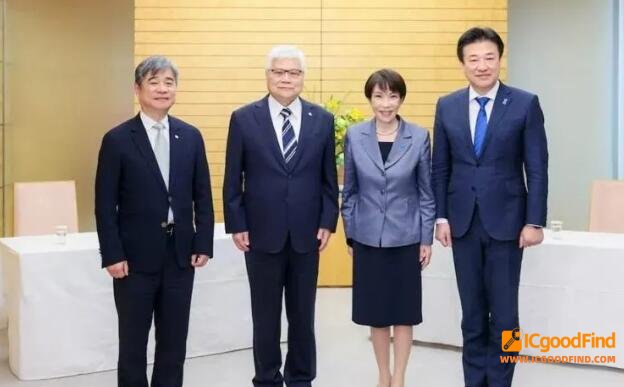
TSMC Chairman C.C. Wei met with Japanese Prime Minister Naomi Koshi to discuss plans to upgrade the company's second fab in Kumamoto, Japan, to 3nm process technology. The Japanese government indicated it would consider providing additional financial support to advance this strategic project.

In an official statement, Wei emphasized that the potential upgrade is a direct response to robust global chip demand driven by AI. TSMC is currently evaluating the feasibility of producing 3nm chips at the Kumamoto site, while expressing gratitude for the sustained support from Japanese authorities.
Originally, the second Kumamoto fab was planned for 6-12nm chip production with a $12.2 billion investment. Due to weaker-than-expected demand for that node and the surge in AI requirements, TSMC paused construction to reconsider its plans. The upgrade to 3nm would raise the total investment to approximately $17 billion. Japan had already committed up to ¥732 billion in subsidies for the second fab and is now assessing the need for further funding for the more advanced node.

The Japanese government clarified that this project complements, rather than competes with, Rapidus's domestic 2nm ambitions, aiming to strengthen the country's overall semiconductor ecosystem.
ICgoodFind : Upgrading the Kumamoto fab to 3nm is a strategic move by TSMC to capture AI-driven demand while supporting Japan's goal of building a more advanced domestic semiconductor supply chain.