
On July 15, Tower Semiconductor announced a ¥600 billion (approx. RMB 25.1 billion) investment in Japan to expand silicon photonics, SiGe, and advanced optical packaging capacity. The project is eligible for up to ¥160 billion in government subsidies under Japan’s Economic Security Promotion Act.
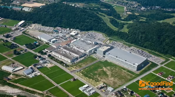
The expansion has two pillars:
A new 12-inch wafer fab adjacent to its existing Fab 7 in Uozu, Toyama Prefecture, to boost silicon photonics and SiGe manufacturing capacity for AI-driven optical interconnect demand.
A conversion of Fab 6 in Myoko, Niigata Prefecture, into a 12-inch silicon photonics production and advanced packaging hub, with full production targeted for Q4 2027.
From ICgoodFind: Photonics is the bandwidth bottleneck – and Tower just placed a giant bet. ¥600B in Japan tells you optical I/O is now a foundry-scale business.
